
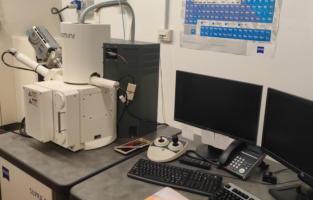
Scanning electron microscopes (SEM) reveal morphology and composition of materials and nanostructures. Our ZEISS SUPRA 40 SEM-FEG provides high-resolution imaging of materials and nanostructures, revealing both their morphology and composition. Thanks to its field-emission cathode, the system delivers exceptional spatial resolution while minimizing sample charging and damage—making it ideal for non-conductive samples and soft matter systems.
The integrated GEMINI column features an ultra-low magnetic field outside the objective lens, enabling precise analysis of magnetic materials and devices. Additionally, the instrument operates effectively at very low beam currents, ensuring high-quality imaging with minimal impact on sensitive samples.
- Nominal resolution: 1.5 nm at 10 KV and WD = 2 mm
- Acceleration voltage: 0.1 KV – 20 KV
- Probe current: 4 pA – 10 nA
- Magnification: 12X – 900KX
- Working distance (WD): from 1mm up to 20 mm, depending on the operating conditions
- Sample size: up to 9 sample of area 1cm2, or a large sample up to 20cm2
Microanalysis EDX
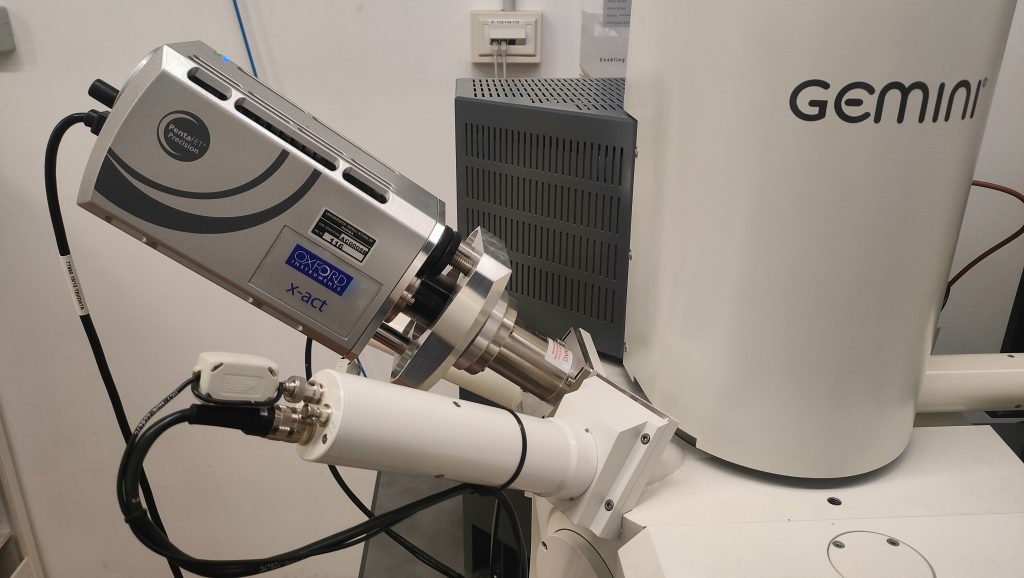
The microscope is equipped with an X-Act Silicon Drift Detector LN2-free (Oxford Instruments) to detect and analyze X-rays emitted by the sample under the electron beam.
It can detect also light elements, from Be onwards, with the excellent energy resolution of 125 eV. The stability is guaranteed from 1.000 to 100.000 cps (resolution change < 1 eV).
Cathodoluminescence
Cathodoluminescence (CL)—the emission of light from a material irradiated by an electron beam—offers complementary insights to standard SEM imaging, especially for nanostructured materials such as semiconductors and metallic nanoparticles. This technique enables the investigation of optical properties, defects, bandgap variations, and local electronic structure, often invisible in conventional electron microscopy.
Our ZEISS SUPRA 40 SEM-FEG is equipped with a light guide and photomultiplier (Zeiss), allowing us to acquire CL signals and spatial maps from a wide range of samples, including semiconductor films, heterostructures, and thin layers.